
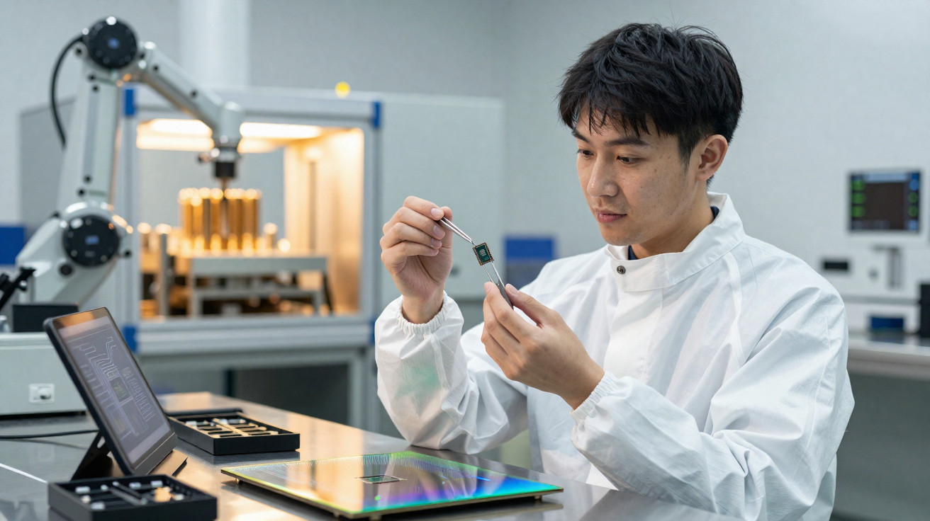
On 1 April 2025, Taiwanese chipmaker TSMC unveiled what it described as the world’s most advanced microchip: a 2 nanometre (2nm) chip.
TSMC expects mass production to begin in the second half of the year, and says the new process marks a significant leap in both performance and efficiency-one that could materially alter the wider technology landscape.
TSMC’s 2nm chip and how microchips work
Microchips underpin modern life and are built into almost every electronic product, from electric toothbrushes and smartphones to laptops and everyday household appliances. They are produced by layering and etching materials such as silicon to form microscopic circuitry containing billions of transistors.
Transistors function as minuscule switches that control electrical current and make computation possible. Broadly speaking, the higher the transistor count on a chip, the faster and more capable it tends to be.
The semiconductor industry continually tries to squeeze more transistors into less space, which is how devices become quicker, more powerful and more energy efficient over time.
What 2nm means versus 3nm: speed, power and density
Set against the previous leading-edge generation-often referred to as 3nm chips-TSMC’s 2nm technology is expected to bring clear gains. TSMC indicates it should offer either a 10%-15% increase in computing speed at the same power level, or a 20-30% cut in power consumption at the same speed.
On top of that, 2nm transistor density is said to rise by around 15% compared with 3nm. In practical terms, this higher density should help devices run faster, use less energy and handle more complex workloads efficiently.
Taiwan, TSMC and the "silicon shield"
Taiwan’s chip sector is closely linked to the island’s security. It is sometimes called the "silicon shield", because its global economic importance is seen as motivating the US and its allies to protect Taiwan against the risk of a Chinese invasion.
Against this backdrop, TSMC has recently agreed a US$100 billion deal (£76 billion) to build five new factories in the US. Even so, it is not yet clear whether 2nm chips can be made outside Taiwan, as some officials worry that shifting cutting-edge production overseas could weaken the island’s security position.
TSMC-short for Taiwan Semiconductor Manufacturing Company-was founded in 1987 and operates as a contract manufacturer, producing chips for other firms. Taiwan represents 60% of the global "foundry" market (outsourced semiconductor manufacturing), and TSMC accounts for the vast majority of that share.
Who uses TSMC chips and how the process has progressed
TSMC’s most advanced chips are deployed across a wide range of products made by other companies. It builds Apple’s A-series processors used in iPhones, iPads and Macs, and it makes NVidia’s graphics processing units (GPUs) used in machine learning and AI workloads.
It also produces AMD’s Ryzen and EPYC processors used by supercomputers around the world, and it manufactures Qualcomm’s Snapdragon processors, which are used in phones from Samsung, Xiaomi, OnePlus and Google.
In 2020, TSMC began a specialised miniaturisation approach known as 5nm FinFET technology, which proved crucial for progress in smartphones and high-performance computing (HPC). HPC refers to getting multiple processors to operate in parallel on demanding computational problems.
Two years on, TSMC introduced a 3nm miniaturisation process using even smaller features, further improving performance and power efficiency. Apple’s A-series processor, for instance, is built on this technology.
Where 2nm chips could have the biggest impact
If smartphones, laptops and tablets adopt 2nm chips, they could see stronger performance alongside improved battery life. That combination could support thinner and lighter designs without giving up computing power.
With greater efficiency and speed, 2nm chips could also strengthen AI-driven uses such as voice assistants, real time language translation and autonomous computer systems (designed to operate with little to no human input).
Data centres may benefit too, through lower energy demand and better processing capability-both of which support wider environmental sustainability goals.
Industries such as autonomous vehicles and robotics could gain from the increased speed and reliability promised by the new chips, potentially making these technologies safer and more viable for large-scale adoption.
The challenges: manufacturing complexity, heat and materials
All of this sounds highly encouraging, but despite being a major milestone, 2nm chips also bring difficulties-starting with the complexity of manufacture.
Making 2nm chips relies on leading-edge methods such as extreme ultraviolet (EUV) lithography. Because the process is both intricate and costly, it drives up production expenses and requires exceptionally high precision.
Heat is another major concern. Even if overall consumption is lower, shrinking transistors and increasing their density makes heat dissipation a critical engineering challenge.
Excess heat can reduce performance and shorten a chip’s lifespan. And at this scale, established materials such as silicon may be pushed towards their limits, which could mean other materials need to be explored.
Even so, the improved computing power, energy efficiency and miniaturisation made possible by these chips could open the door to a new phase of consumer and industrial computing.
Smaller chips may unlock breakthroughs in future technologies, enabling devices that are not only powerful but also discreet and more environmentally friendly.
Domenico Vicinanza, Associate Professor of Intelligent Systems and Data Science, Anglia Ruskin University
This article is republished from The Conversation under a Creative Commons licence. Read the original article.






Comments
No comments yet. Be the first to comment!
Leave a Comment